Infineon IRFR4510TRPBF Power MOSFET: Key Specifications and Application Circuit Design
The Infineon IRFR4510TRPBF is a widely adopted N-channel power MOSFET that excels in a variety of switching applications. Its robust performance and cost-effectiveness make it a popular choice for designers working on power supplies, motor controls, DC-DC converters, and high-side switches. Understanding its key specifications is fundamental to implementing a reliable and efficient application circuit.
Key Specifications
The IRFR4510TRPBF is built on Infineon's advanced technology platform, offering a compelling set of electrical characteristics:
Drain-Source Voltage (VDS): 100 V. This rating makes it suitable for a broad range of applications operating at common bus voltages like 24V, 48V, and even higher with sufficient safety margin.
Continuous Drain Current (ID): 12 A at a case temperature (TC) of 25°C. This high current handling capability allows it to drive substantial loads directly.
On-Resistance (RDS(on)): A remarkably low 62 mΩ (max.) at VGS = 10 V. This is a critical parameter as it directly determines the conduction losses (I²R) of the MOSFET when switched on. A lower RDS(on) means higher efficiency and less heat generation.
Gate Threshold Voltage (VGS(th)): Typically 2.0V to 4.0V. This standard threshold voltage ensures easy drive compatibility with common logic-level and microcontroller outputs when used with a suitable gate driver.
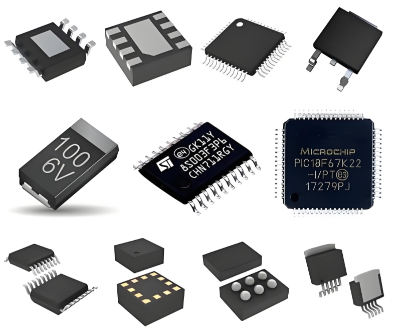
Package: TO-252 (DPAK). This surface-mount package offers an excellent balance between power dissipation capability and board space savings, providing a low thermal resistance from junction to case (RθJC = 1.7 °C/W).

Application Circuit Design: A DC Motor Driver
A common application for the IRFR4510TRPBF is a simple yet effective low-side switch for a DC motor. The core circuit consists of the MOSFET, a microcontroller (MCU), a gate driver, and essential protection components.
1. Gate Driving: While the MCU can turn the MOSFET on, its output current is often limited. Using a dedicated gate driver IC (e.g., TC4427) between the MCU and the MOSFET's gate is highly recommended. This driver rapidly charges and discharges the MOSFET's inherent gate capacitance, ensuring fast switching transitions. Fast switching minimizes the time spent in the high-loss linear region, significantly reducing switching losses and preventing thermal runaway.
2. Gate Resistor (RG): A small series resistor (e.g., 10-100 Ω) at the gate is crucial. It damps high-frequency oscillations that can occur due to parasitic inductance and the MOSFET's Miller capacitance, preventing electromagnetic interference (EMI) and potential gate voltage overshoot.
3. Flyback Diode (D1): An inductive load like a motor generates a large voltage spike when the current is suddenly interrupted (when the MOSFET turns off). This spike can easily exceed the MOSFET's VDS rating and destroy it. A flyback diode (Schottky or fast-recovery) is placed in reverse bias across the motor. It provides a safe path for the inductive current to decay, clamping the voltage spike and protecting the MOSFET.
4. Pull-Down Resistor (RPD): A high-value resistor (e.g., 10 kΩ) from the gate to ground is essential. It ensures the MOSFET remains firmly off if the MCU pin is in a high-impedance state (e.g., during startup or reset), preventing false triggering from external noise.
Design Considerations:
Heat Sinking: Calculate the total power dissipation (PD = ID² RDS(on) + Switching Losses). If necessary, attach a suitable heatsink to the DPAK tab to keep the junction temperature within safe limits.
Layout: Minimize parasitic inductance in the high-current loop (source-drain) and the gate drive loop. Use short, wide traces and place decoupling capacitors close to the MOSFET.
ICGOOODFIND: The Infineon IRFR4510TRPBF is a versatile and robust power MOSFET, prized for its high voltage rating, low on-resistance, and high current capacity. Successful implementation hinges on thoughtful circuit design, particularly robust gate driving, effective protection against inductive kickback, and proper thermal management to fully leverage its performance potential in switching applications.
Keywords: Power MOSFET, Low On-Resistance, Gate Driver, Flyback Diode, Switching Application.
